
PCB manufacturing service
PCB Manufacturing: Fabrication and Assembly
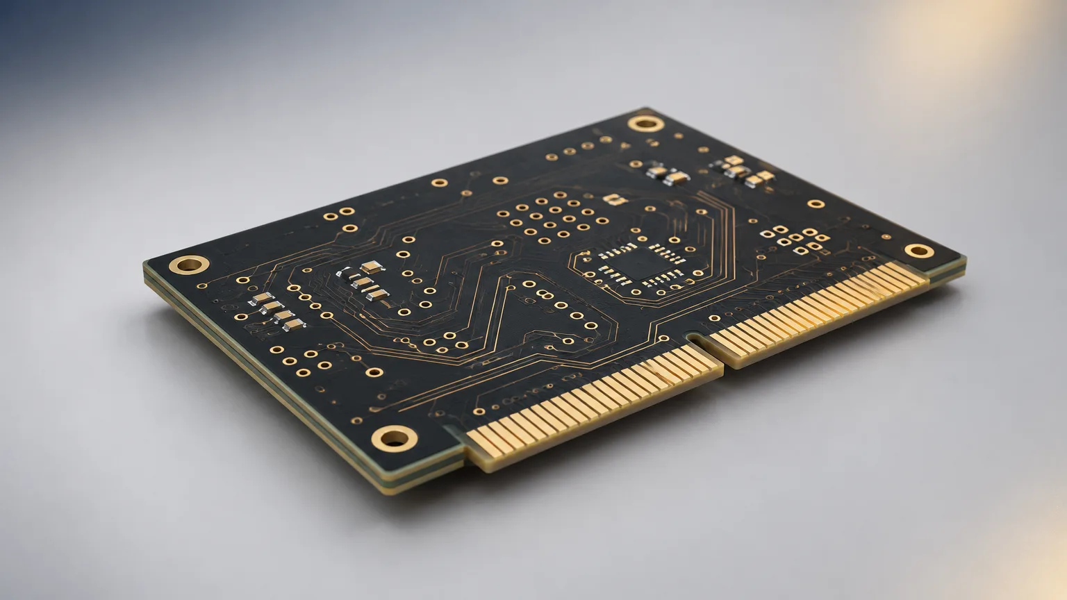
PCB manufacturing covers bare-board fabrication and component assembly. Sourcing Repository collects quotes from a vetted supplier network, manages quality and inspection, and delivers finished boards to your drawing.
- SMT, THT and mixed technology
- Prototype to production volume
- IPC-based inspection
- One point of contact
- Quote turnaround5-7 working days from complete data
- Inspection to IPC-A-610Class 1, 2 or 3 acceptance criteria
- Gerber, BOM, pick-and-placeControlled revisions required
PCB manufacturing combines two stages: fabrication, which produces the bare printed circuit board, and assembly, which attaches and solders components to create a working circuit-board assembly. Sourcing Repository is a manufacturing broker that collects quotes from a vetted supplier network, manages inspection and testing, and delivers finished boards.
What PCB manufacturing is and when to use it
PCB manufacturing is the combined service of fabricating a bare printed circuit board and assembling electronic components onto it to produce a functional circuit-board assembly. Fabrication creates the board structure and conductive features; assembly installs and solders the components.
The service suits engineering teams and procurement managers who need boards built to a controlled revision rather than a single prototype. It covers prototypes, low-volume production and high-volume manufacturing, and it applies whenever a design must move from files to tested hardware.
When to use a PCB manufacturing service
- You have released Gerber or board data plus a bill of materials (BOM) and need boards built.
- Your design mixes surface-mount technology (SMT) and through-hole technology (THT) parts.
- You need documented inspection and electrical testing, not just populated boards.
- You want one supplier accountable for fabrication, assembly and test rather than several.
- You are scaling from prototype quantities to repeatable production runs.
PCB fabrication and assembly process steps
The PCB fabrication and assembly process runs from data review to tested boards, and the route depends on whether the design is SMT, THT, mixed technology or thermal-assisted through-hole (THR). Printed circuit board assembly (PCBA) is the stage that installs and solders components on the fabricated board.
- 1. Data review and DFM feedback The supplier checks board data, the BOM, pick-and-place coordinates and assembly drawings against the specification, and returns manufacturability questions before tooling starts.
- 2. Bare-board fabrication The bare PCB is produced from the fabrication drawing: conductive layers, plated holes, solder mask and surface finish. The drawing defines board dimensions and hole locations, with IPC-2221C giving generic design requirements.
- 3. Stencil and paste printing (SMT) A stainless-steel stencil controls solder-paste deposit location and volume. Paste is printed onto the pads and inspected, often with solder-paste inspection (SPI).
- 4. Component placement Feeder-based machines place surface-mount components. Placement accuracy is machine- and package-dependent and is confirmed against the assembly drawing.
- 5. Reflow soldering The board passes through a controlled thermal profile that melts the paste and forms the solder joints. The profile depends on the alloy, components and assembly design.
- 6. Through-hole insertion and soldering THT leads are inserted through plated holes and joined by wave soldering, selective soldering or hand soldering. THR instead presses paste into plated holes before placement and reflow, reducing process stages.
- 7. Cleaning and inspection Boards are cleaned where the process requires it, then checked by automated optical inspection (AOI) and visually against IPC-A-610J Class 1, 2 or 3 criteria for placement and solder defects.
- 8. Electrical test and packout Continuity, isolation and functional limits follow the customer test specification, using in-circuit test (ICT), flying probe or functional test. Passed boards are serialized where required and packed for shipment.
PCB materials and surface finishes
PCB materials and surface finishes are set by the fabrication drawing and the assembly process. The table lists material families commonly used in rigid board fabrication and soldering.
| Material | Grade | Properties | Typical uses |
|---|---|---|---|
| FR-4 laminate | Grade must be specified by fabricator; exact grade unverified | Glass-reinforced epoxy laminate; electrical insulation and structural support | Rigid single-sided, double-sided and multilayer PCBs |
| Copper foil | Exact foil weight unverified | Conductive layer used for traces, pads, planes and plated features | All conventional rigid PCB constructions |
| SAC305 solder paste | SAC305 lead-free alloy | Tin-silver-copper solder alloy suspended with flux; Intel identifies SAC305 and SAC405 as lead-free paste options | RoHS-oriented SMT reflow assembly |
| SAC405 solder paste | SAC405 lead-free alloy | Tin-silver-copper solder alloy with flux; thermal profile depends on paste and assembly design | Lead-free SMT reflow |
| Tin-lead solder | Exact alloy unverified | Lower-temperature solder option; composition and regulatory suitability must be specified | Permitted industrial, aerospace, legacy or exempt applications |
| Solder-mask polymer | Exact chemistry unverified | Insulates and protects copper while exposing solderable pads | Rigid and flexible PCB surface protection |
| Stainless-steel stencil | Laser-cut or electroformed grade unverified | Controls solder-paste deposit location and volume | SMT paste printing; nickel-alloy alternatives are also reported |
| Component materials | Part-specific | Semiconductor packages, ceramic capacitors, resistors, connectors and electromechanical parts | Circuit functions, interconnection, sensing, power conversion and control |
Surface finish comes from the fabrication drawing. State the finish, laminate grade and copper weight explicitly, because a Gerber file alone does not carry them.
PCB manufacturing specifications and tolerances
PCB manufacturing specifications and tolerances are set mostly by supplier capability and your drawing, not by a single industry number. The table lists the parameters to fix before a quote is final.
| Parameter | Typical range | Standard or source |
|---|---|---|
| Component placement accuracy | Unverified; machine- and package-dependent | Supplier capability and assembly drawing |
| Solder-paste deposit volume | Unverified; controlled by stencil, aperture, paste and SPI limits | Process specification; SPI program |
| PCB dimensions and hole locations | Unverified; defined by fabrication drawing | IPC-2221C provides generic printed-board design requirements |
| Solder-joint acceptability | Class 1, 2 or 3 acceptance criteria | IPC-A-610J visual acceptability standard |
| Soldering process requirements | Alloy-, component- and profile-dependent | IPC J-STD-001J |
| Board warpage | Unverified; fabrication and assembly specification required | Supplier drawing and applicable IPC acceptance criteria |
| Electrical test limits | Product-specific continuity, isolation and functional limits | Customer test specification; ICT, flying probe or functional test |
Lead time depends on data completeness, tooling, component availability, test method and quantity. Confirm the schedule against your build plan before release.
DFM tips that lower PCB assembly cost
Design for manufacturing (DFM) decisions made before release usually cost less to change than process fixes made after tooling. These seven points address the most common cost drivers.
- Standardize the BOM: fewer unique part numbers mean fewer feeder setups, fewer reels and less changeover time.
- Keep components on one side where possible. Single-sided assembly avoids a second pass, second stencil and extra handling.
- Use SMT for high-count parts. SMT is often lower cost at volume because of automation, while THT adds drilling, insertion and soldering steps.
- Reserve THT for parts that need mechanical retention, then group those joints so wave or selective soldering is efficient.
- Design panel-friendly board sizes and add rails and fiducials so placement and inspection equipment can locate the board reliably.
- Match pad and aperture geometry to the paste-printing process; paste deposit volume is controlled by stencil, aperture, paste and SPI limits.
- State the acceptance class and test method up front. IPC-A-610J Class 1, 2 or 3 and the choice of ICT, flying probe or functional test change inspection and fixture effort.
Typical PCB assembly applications
PCB manufacturing supports control, sensing, power and communication functions across several industries. The examples below show where each assembly route is normally chosen.
- Automotive control modules: dense SMT boards with mixed-technology connectors, built to automotive acceptance criteria.
- Industrial controllers and drives: mixed-technology boards where power components need through-hole retention.
- Sensors and instrumentation: small SMT assemblies with tight placement requirements and functional test.
- Power conversion boards: assemblies combining surface-mount control circuitry with through-hole magnetics and terminals.
- Communications and networking hardware: high-density SMT boards with serialized testing.
- Prototype and pilot builds: manual placement and hand soldering with flying-probe or functional testing, used to validate a design before tooling.
Prototype assembly
- Low tooling cost
- Manual placement and hand soldering
- Flying-probe or functional testing
- Slower and less repeatable at volume
Production assembly
- Feeder-based placement and reflow
- Automated inspection
- Serialized testing
- Setup, tooling and programming costs apply
What drives PCB manufacturing cost
PCB manufacturing cost is the sum of the board, the components and the process effort around them. No single factor dominates, and the mix changes between prototype and production quantities.
- Components: part count, package mix, sourcing route and lifecycle status.
- Placement: number of placements, board area and whether assembly is single- or double-sided.
- Soldering: reflow only, or added wave, selective or hand soldering for through-hole joints.
- Setup and tooling: stencils, programming, fixtures and panel design.
- Inspection and test: visual acceptance class, SPI, automated inspection, and ICT, flying probe or functional test.
- Labor and secondary operations: rework, cleaning, conformal coating, depanel and packout.
- Yield and freight: expected fallout on complex builds, plus shipping and delivery location.
Cost is calculated from the data you supply, so incomplete BOM attributes or an unstated test requirement usually return as a quote revision rather than a firm number.
Why order PCB manufacturing through Sourcing Repository
Ordering PCB manufacturing through Sourcing Repository gives you one managed route to fabricated and assembled boards. Sourcing Repository is a manufacturing broker: it does not own factories or machines, but collects quotes from a vetted supplier network, manages quality and inspection, and delivers the finished parts.
- Vetted supplier network: suppliers are matched to your board type, volume and acceptance class.
- One point of contact: a single contact covers fabrication, assembly, inspection and delivery.
- Managed quality and inspection: acceptance criteria and test requirements are carried into the order and checked at inspection.
- Quote turnaround: typically 5-7 working days from complete, controlled data.
Send your Gerber or board data, BOM, pick-and-place coordinates, assembly drawing, quantities and test requirements to killol@sourcingrepository.com to start a quote. Sourcing Repository operates from 201 SG Mall, Ahmedabad.
Have a drawing to quote?
Upload it with quantity and material to start a quote.
FAQ
Common questions
Does PCB assembly include bare-board fabrication?
Not necessarily. Assembly-only and consigned orders assume you supply the bare boards or components. Request a turnkey quote if the supplier must source fabricated PCBs, components, assembly, inspection and testing under one scope.
How is PCB assembly cost calculated?
It combines components, placement, soldering, setup, tooling, inspection, testing, labor, secondary operations, freight and expected yield. The balance shifts with quantity, so prototype and production quotes are rarely built the same way.
What files are needed for a PCB assembly quote?
A supplier usually needs the BOM, board data, pick-and-place coordinates, assembly drawings, revision information, quantities, test requirements and component sourcing instructions. Controlled revisions and complete BOM attributes reduce the number of quote revisions.
Can the assembler source components?
Yes. Many suppliers offer turnkey component sourcing, but they typically require approved manufacturers, alternates, authenticity controls, lifecycle review and your approval before any parts are ordered. Consigned assembly is the alternative if you supply the components.
Related resources
Keep reading
Ready when you are
Send your PCB data for a quote
Share your Gerber or board data, BOM, pick-and-place coordinates, assembly drawing, quantities and test requirements. Sourcing Repository returns quotes from a vetted supplier network in 5-7 working days.
Your files stay confidential. NDA available on request.