
PCB Assembly Service
PCB Assembly (PCBA) for Prototypes and Production
PCB assembly attaches electronic components to a fabricated bare board to create a working circuit-board assembly.
- SMT, THT and mixed technology
- Prototype to high volume
- IPC-A-610J inspection
- One point of contact
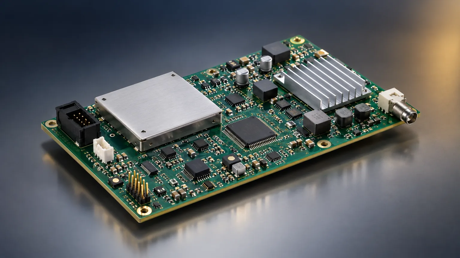
- Surface-mount assemblyStencil print, place, reflow, inspect
- Through-hole assemblyWave, selective or hand soldering
- Electrical testingFlying probe, ICT or functional test
PCB assembly is the process of attaching electronic components to a fabricated printed circuit board to create a functional circuit-board assembly. It combines surface-mount technology, through-hole technology, soldering, inspection and electrical testing. PCB assembly supports prototypes, low-volume production and high-volume manufacturing for control boards, power electronics, communications and embedded systems.
What PCB Assembly Is and When to Use It
PCB assembly is the process of attaching electronic components to a fabricated printed circuit board (PCB), creating a functional circuit-board assembly. It commonly combines surface-mount technology (SMT), through-hole technology (THT), soldering, inspection and electrical testing.
PCB fabrication produces the bare board; assembly installs and solders components. Buyers who want one supplier for both often ask for PCB manufacturing and assembly, or PCB fabrication assembly.
Who this service is for
- Engineers validating a new circuit board design.
- Procurement managers sourcing repeat builds.
- Founders moving a hardware product from prototype to volume.
- Automotive and industrial teams that need documented inspection and test.
When to use PCB assembly
- You have a bare board (or fabrication data) and a bill of materials (BOM).
- Components must be placed, soldered and electrically tested.
- You need repeatable output across a build quantity, not a one-off hand build.
- You want inspection evidence tied to an acceptance standard such as IPC-A-610J.
PCB Assembly Process Steps
PCB assembly follows one sequence from data review to final test. The steps below describe a typical SMT-led build, with through-hole content added where the design requires it.
- 1. Review documentation and DFM The supplier checks the BOM, board data, pick-and-place coordinates, assembly drawing and revision. Design-for-manufacturing issues are raised before tooling is ordered.
- 2. Source and kit components Components are purchased against the BOM (turnkey assembly) or supplied by the customer (consigned assembly). Part numbers and package types are confirmed before kitting.
- 3. Print solder paste and inspect it A stainless-steel stencil, typically about 0.005 in (0.13 mm) thick, deposits solder paste onto the pads. Stencil, aperture design, paste type and solder-paste inspection (SPI) limits control paste volume.
- 4. Place surface-mount components Feeder-based placement machines position components on the printed pads. Accuracy depends on the machine and package and is set by supplier capability and the assembly drawing.
- 5. Reflow solder Reflow soldering passes the board through a controlled thermal profile that melts the paste and forms the joints. Settings depend on the alloy, components and assembly design.
- 6. Insert and solder through-hole parts Leads are inserted through plated holes and joined by wave, selective or hand soldering. Thermal-assisted through-hole (THR) presses paste into plated holes before reflow, reducing process stages.
- 7. Clean, inspect and rework Boards are cleaned where required, then checked visually and by automated optical inspection (AOI). Solder joints are judged against Class 1, 2 or 3 criteria in IPC-A-610J.
- 8. Test and pack In-circuit test (ICT) uses fixtures for fast, repeatable production testing. Flying-probe test needs less dedicated tooling but is typically slower, so it suits prototypes and low volumes. Limits come from the customer test specification, and passing boards are packed to the agreed delivery requirements.
PCB Assembly Materials and Finishes
Material and finish choices are set by the fabrication drawing and the assembly process specification. The table lists the material families commonly involved in PCB manufacturing and assembly.
| Material | Grade | Properties | Typical uses |
|---|---|---|---|
| FR-4 laminate | Grade must be specified by fabricator; exact grade unverified | Glass-reinforced epoxy laminate; electrical insulation and structural support | Rigid single-sided, double-sided and multilayer PCBs |
| Copper foil | Exact foil weight unverified | Conductive layer used for traces, pads, planes and plated features | All conventional rigid PCB constructions |
| SAC305 solder paste | SAC305 lead-free alloy | Tin-silver-copper solder alloy suspended with flux; Intel identifies SAC305 and SAC405 as lead-free paste options | RoHS-oriented SMT reflow assembly |
| SAC405 solder paste | SAC405 lead-free alloy | Tin-silver-copper solder alloy with flux; thermal profile depends on paste and assembly design | Lead-free SMT reflow |
| Tin-lead solder | Exact alloy unverified | Lower-temperature solder option; composition and regulatory suitability must be specified | Permitted industrial, aerospace, legacy or exempt applications |
| Solder-mask polymer | Exact chemistry unverified | Insulates and protects copper while exposing solderable pads | Rigid and flexible PCB surface protection |
| Stainless-steel stencil | Laser-cut or electroformed grade unverified | Controls solder-paste deposit location and volume | SMT paste printing; nickel-alloy alternatives are also reported |
| Component materials | Part-specific | Includes semiconductor packages, ceramic capacitors, resistors, connectors and electromechanical parts | Circuit functions, interconnection, sensing, power conversion and control |
PCB Assembly Specifications and Tolerances
PCB assembly tolerances are not universal. Supplier machine capability, component package and the acceptance criteria in the purchase specification set them. The table lists each parameter to define and the document that governs it.
| Parameter | Typical range | Standard or source |
|---|---|---|
| Component placement accuracy | Unverified; machine- and package-dependent | Supplier capability and assembly drawing |
| Solder-paste deposit volume | Unverified; controlled by stencil, aperture, paste and SPI limits | Process specification; SPI program |
| PCB dimensions and hole locations | Unverified; defined by fabrication drawing | IPC-2221C provides generic printed-board design requirements |
| Solder-joint acceptability | Class 1, 2 or 3 acceptance criteria | IPC-A-610J visual acceptability standard |
| Soldering process requirements | Alloy-, component- and profile-dependent | IPC J-STD-001J |
| Board warpage | Unverified; fabrication and assembly specification required | Supplier drawing and applicable IPC acceptance criteria |
| Electrical test limits | Product-specific continuity, isolation and functional limits | Customer test specification; ICT, flying probe or functional test |
Design Tips That Lower PCB Assembly Cost
Most assembly cost is decided before the quote is issued. These design choices reduce setup, tooling, labor and rework across PCB fabrication and assembly.
- Standardize the BOM. Fewer unique part numbers reduce feeder setup, kitting labor and the risk of sourcing delays.
- Keep to one assembly side where possible. Single-sided SMT avoids a second print, place and reflow pass.
- Use the largest package that meets the design. Fine-pitch and small packages raise placement and inspection demands.
- Minimize through-hole content. THT adds drilling, insertion and wave, selective or hand soldering steps; THR can cut process stages when components and hole design allow.
- Design panel-friendly board outlines and add clear fiducials and tooling holes so placement and test fixtures are simpler.
- Specify the acceptance class and test method up front. Naming IPC-A-610J Class 1, 2 or 3 and the test type prevents rework and quote revisions.
- Control revisions. Frozen board data, BOM and pick-and-place files avoid re-quotes and duplicate tooling.
Typical PCB Assembly Applications
PCB assembly is used wherever a bare board must become an operating electronic assembly. Common examples include control boards, power electronics, communications equipment and embedded systems.
- Automotive control and sensor boards, built to the acceptance class and test plan the program requires.
- Industrial motor drives, power supplies and power-conversion boards.
- Communications and networking boards with dense surface-mount content.
- Embedded controllers, instrumentation and data-acquisition boards.
- Prototype and pilot builds used to validate a design before volume release.
Prototype and low volume
- Manual placement and hand soldering where suitable
- Low tooling cost
- Flying-probe or functional testing
- Slower and less repeatable at volume
Automated production
- Feeder-based placement and reflow
- Automated inspection and serialized testing
- Repeatability and throughput
- Setup, tooling and programming costs apply
What Drives PCB Assembly Cost
PCB assembly cost is the sum of the inputs a build consumes, not a single rate. The list below shows the factors that move price most, so you can compare quotes on the same basis.
- Components: part cost, availability, minimum packaging and sourcing route (turnkey or consigned).
- Placement count and package mix: total placements, fine-pitch content and odd-form parts.
- Process route: SMT only, THT only, mixed technology or THR, each with different stage counts.
- Setup and tooling: stencil, programming, feeders and any test fixture.
- Inspection and test: visual and automated inspection, flying probe, ICT or functional test.
- Labor and secondary operations: hand soldering, cleaning, conformal coating, depanel and packing.
- Yield and rework: expected fallout from paste, placement and thermal-profile control.
- Logistics: freight, delivery location and schedule pressure.
Why Order PCB Assembly Through SR
Ordering PCB assembly through SR gives you one quote from a vetted supplier network, with quality and inspection managed for you. SR is a manufacturing broker and does not own factories or machines.
- Vetted supplier network: suppliers are matched to your board type, volume and test requirements.
- One point of contact: you send one set of files and receive one consolidated quote.
- Quote turnaround: typically 5-7 working days from complete documentation.
- Quality and inspection management: acceptance class, inspection method and test plan are agreed before the build.
- Delivery management: SR tracks the build and ships finished assemblies to your location.
Have a drawing to quote?
Upload it with quantity and material to start a quote.
FAQ
Common questions
Does PCB assembly include bare-board fabrication?
Not necessarily. PCB fabrication produces the bare board, while assembly installs and solders components. Request a turnkey quote if the supplier must source the fabricated PCBs, components, assembly, inspection and testing as one scope.
What files are needed for a PCB assembly quote?
A PCB assembly quote usually needs the BOM, board data, pick-and-place coordinates, assembly drawings and revision information. Also include quantities, test requirements and component sourcing instructions. Complete, revision-controlled files reduce quote revisions.
How is PCB assembly cost calculated?
PCB assembly cost combines components, placement, soldering, setup, tooling, inspection, testing, labor, secondary operations, freight and expected yield. Package mix and quantity shift these inputs, so the price is confirmed per project in the quote.
Which is cheaper, SMT or THT?
SMT is often lower cost at volume because of automation. Actual cost depends on package mix, placement count, tooling, board design and any THT requirements, so compare quotes built from the same BOM and drawings.
Related resources
Keep reading
Ready when you are
Get a PCB assembly quote
Send your BOM, board data and test requirements. SR collects quotes from a vetted supplier network, manages quality and inspection, and delivers finished assemblies.
Your files stay confidential. NDA available on request.